Fluke 8050A Hardware
The Fluke 8050A Multimeter LCD Display Project replaces the display in my Fluke 8050A Desktop DMM with a TFT LCD bitmapped display.
Hardware
The intent of the project is to replace the ancient 4½ digit LCD display on the Fluke 8050A multimeter with an ILI9341 based 320x240 pixel color graphical LCD display. This just about perfectly fits within the cut-out in the front panel of the device where the old 4 digit LCD mounted in a bezel is present. The intent is to both display additional information (such as the mode of the meter - Volts, Amps, Ohms, etc) and larger and easier to read numerical display of the measured values.
Theory of Operation
The Fluke 8050A Theory of Operation page describes the Fluke 8050A and how that drives the requirements for the STM32F103 microcontroller used to drive the ILI9341 TFT LCD graphics display.
The general approach is that the microcontroller monitors the current option of the Fluke 8050A to render a graphical display on the 320x240 TFT LCD.
STM32F103 microcontroller
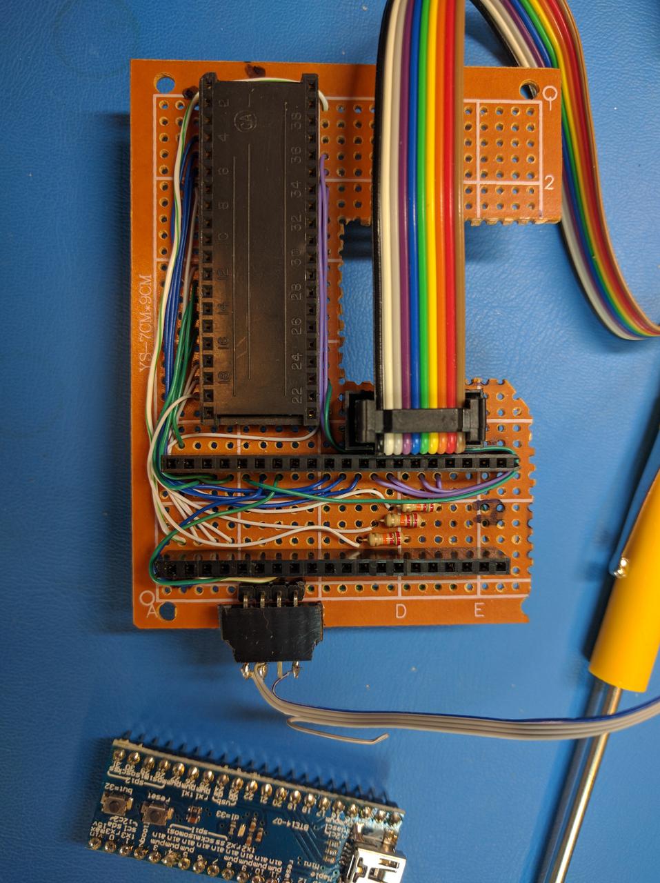
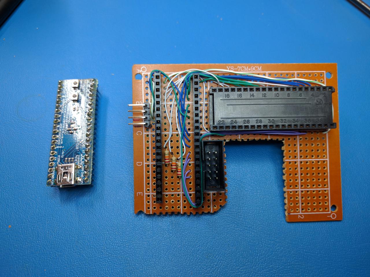
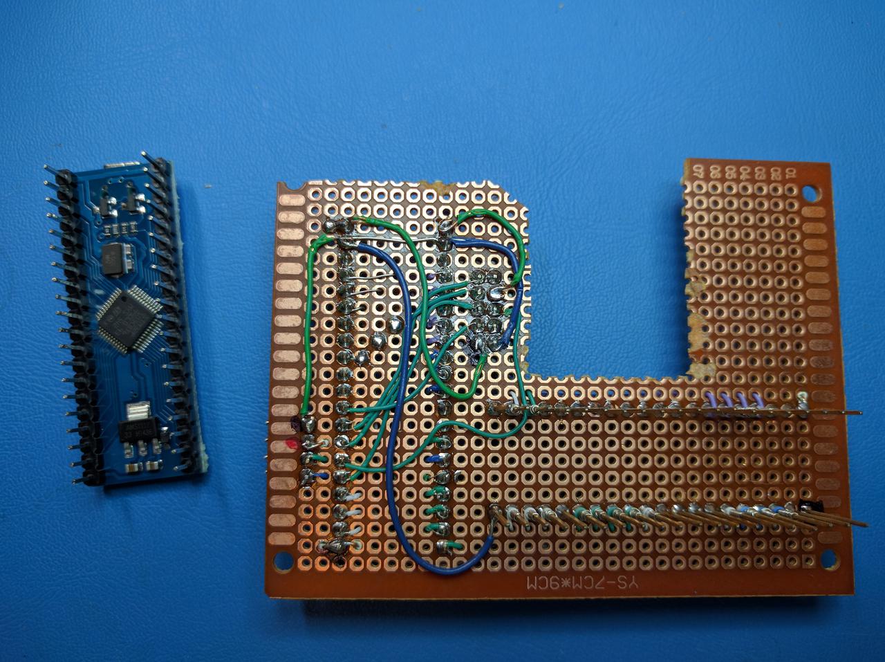
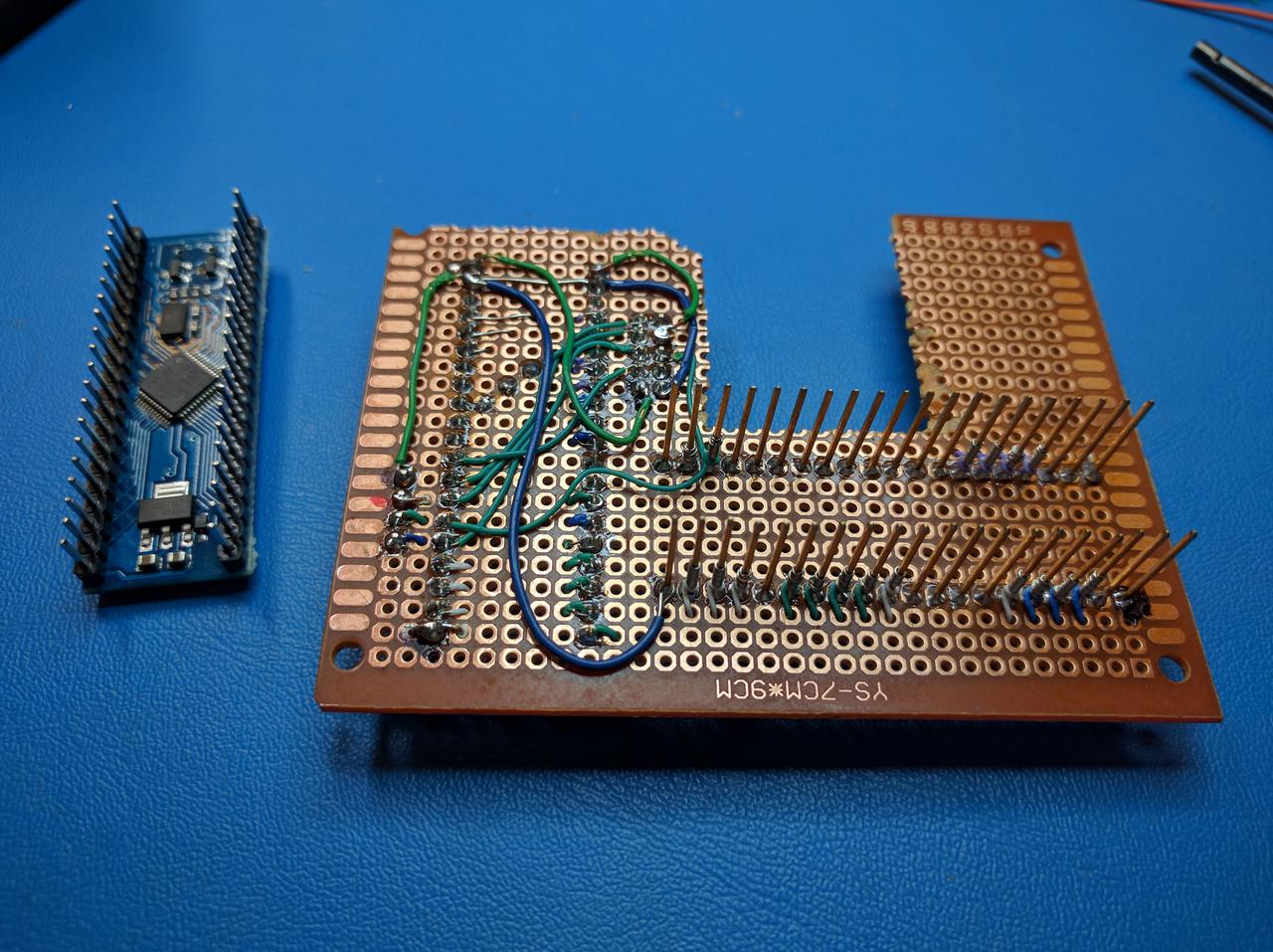
The basis of the extension used to drive the graphical LCD display is an STM32F103 microcontroller. In this implementation, I've chosen to use an inexpensive "Maple Mini" clone device which has an STM32F103CBT6 device on a small carrier board in a 40 pin DIP form factor.
There are a variety of I/O pins available, and their specific assignment for use is documents on the STM32F103 I/O pin assignments page. Note that not all the pins on this device are 5 volt tolerant, so the pin assignment is done with that in mind. If I were to do it over, I likely would have chosen a different specific product with more I/O pins available to allow for additional flexibility in choosing I/O pin assignment and having additional resources available for other uses..
Note that 3 of the signals have 22K resistors in series to limit the current to non 5V tolerant GPIO pins. This value isn't critial.
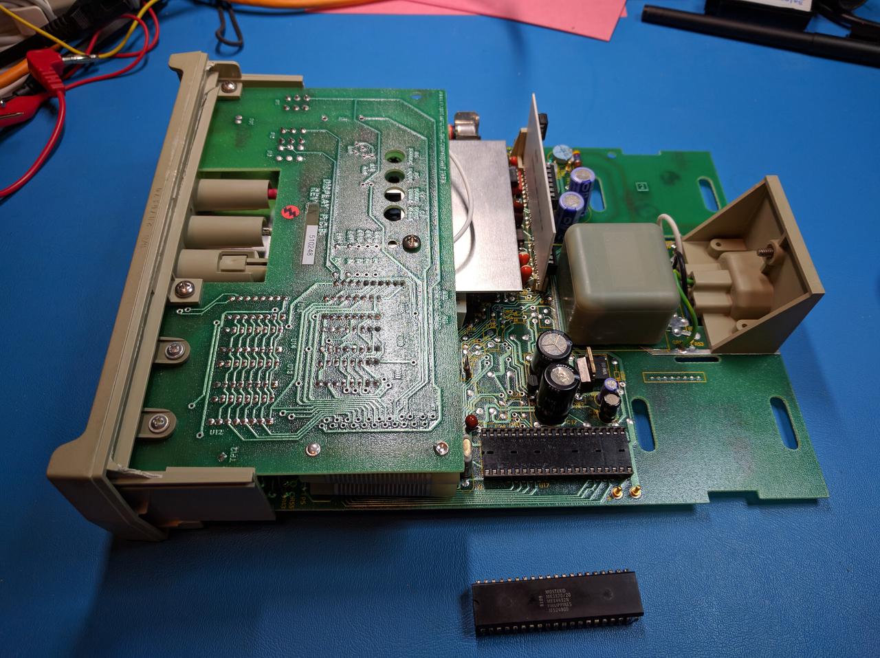
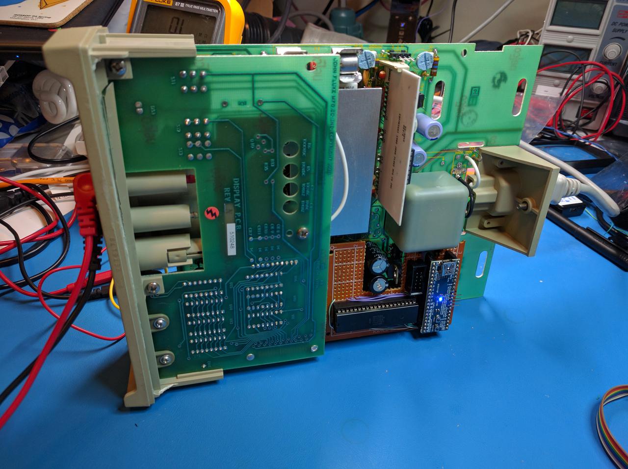
Quite a few signals on the Fluke's 3870 microprocessor need to be connected to. Initially, I had contemplated simply soldering a number of small #30 AWG "wire-wrap" wire to socket pins on the bottom side of the Fluke PCB. However, this was a permanent modification, which I was trying to avoid. Further, I had purchased another cheap Fluke 8050A via EBay that had "some issues" (looks like some mechanical damage due to something heaving being dropped on it. While a little squirrely on on particular range, it worked well enough to serve as a development platform to avoid putting my working 8050A at risk. So being able to move the completed work easily from the development platform to another unit was desirable.
So instead a circuit was constructed on a small prototyping board. It included a 2 20 pin headers to accept the Maple Mini board, and a 40 pin "wire-wrap" style socket which has long pins. The 3870 CPU was removed from its socket, and the wire wrap socket pins are plugged into the Fluke's socket and the 3870 CPU inserted into the wire-wrap socket. This now provides easy access to all the signals on the Fluke's 3870 CPU (including Ground and -5V DC for power).
I/O pin signal levels
The STM32F103CBT6 microprocessor has some number of 5 volt tolerant I/O pins available, while primarily operating with 3.3 volt logic levels. As the logic in the Fluke 8050A is all at 5 volt levels, we utilize 5 volt tolerant GPIO pins quite extensively. Note that even with the 5v tolerant I/O pins, the STM32F103CBT6 data sheet recommends disabling pull-up and pull-down resistors in the specifications for the I/O pins:
- FT = 5V tolerant. To sustain a voltage higher than VDD+0.5 the internal pull-up/pull-down resistors must be disabled.
Still, there are insufficient total 5 volt tolerant GPIO pins available, and there are still a few remaining signals to handle with "normal" GPIO pins. These remaining input signals to the F8 microprocessor are those connected to poles on panel switches used to determine what mode the meter is in. These switches are connected to input pins on the F8 and when closed connect the input ground. Internal F8 pull-ups allow these to float in a high state when the switch is open.
We will use a current limiting resistor in series with the STM32F103 input pin to limit the current drawn. While the pins in question are not 5 volt tolerant, the STM32F103CBT6 data sheet says:
IINJ(PIN) (+/- 5mA) must never be exceeded. This is implicitly insured if VIN maximum is respected. If VIN maximum cannot be respected, the injection current must be limited externally to the IINJ(PIN) value. A positive injection is induced by VIN > VDD while a negative injection is induced by VIN < VSS.
A 22K resistor (just what I had around) with the 5.0V - 3.3V = 1.7V voltage drop yields 77 microamps of current. This value is not critical; even a 2.2K resistor should limit input current to less than 1mA.
Hardware Resources
Some other pages with reference information about the signal assignment from pins on the existing embedded "F8" CPU in the Fluke 8050A and the STM32F103 microcontroller. At some point, a real schematic should be constructed.
Comments